从高速微控制器系列向超高速闪存微控制器的升级
Porting Applications from the High-Speed Micro Family to Ultra-High-Speed Flash Microcontrollers |
Abstract: There are many reasons to upgrade older 8051 designs that use high-speed microcontrollers (DS80C310/DS80C320/DS80C323/DS8xC520) to the newer ultra-high-speed flash microcontrollers (DS89C430/DS89C450). Incentives to upgrade include higher performance, additional features and peripherals, and the flexibility of internal flash memory. This application note discusses some important differences between the two microcontroller families and explains how to upgrade from the high-speed to the ultra-high-speed devices. OverviewMaxim's high-speed microcontroller family includes a wide variety of 8051 microcontrollers which execute instructions at a faster 4 clocks-per-machine-cycle rate compared to the 8051's original 12 clocks-per-machine cycle speed. Some of the high-speed microcontrollers operate entirely from external program memory, such as the DS80C310, while others contain internal EPROM or ROM program memory, such as the DS87C520/DS83C520. All of these high-speed devices are pin-compatible with existing 8051 microcontrollers, so designs can be upgraded in most cases simply by dropping in a faster device and making minor software adjustments.In a similar manner, the ultra-high-speed flash microcontrollers can be used as drop-in upgrades for high-speed microcontroller designs. These newer, more powerful microcontrollers, which include the DS89C430/DS89C450, offer important improvements: expanded internal program flash memory (up to 64kB); and a redesigned, ultra-high-speed microcontroller core capable of executing instructions in a single clock cycle for up to a 12x speed improvement over the original 8051 design. This application note discusses how to upgrade from the high-speed microcontrollers to ultra-high-speed flash devices. The article also outlines differences in feature sets, pinout details, and SFR changes that must be considered when upgrading a design. General ReferencesFor general programming guidelines for the following devices, consult the High-Speed Microcontroller User's Guide (PDF).
Basic Device FeaturesTable 1. Comparison of Device Features
Device Pinout SchemeTable 2. Device Pinout Differences
Device RegistersTable 3. SFR Map Comparisons
Table 4. SFR Function Differences
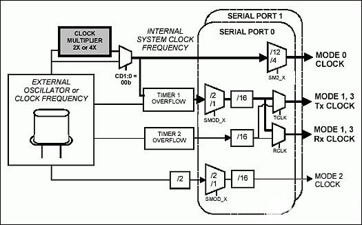
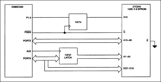
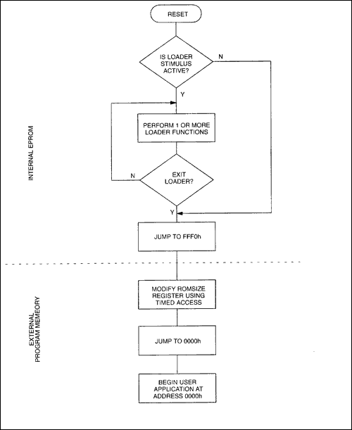
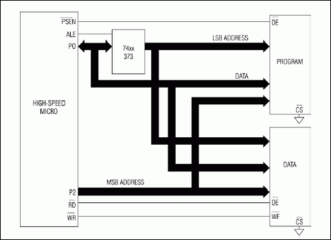
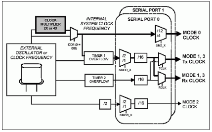
Single-Cycle ExecutionThe ultra-high-speed DS89C430/DS89C450 processors require only a single clock to execute a single-cycle instruction, which is a 4x speed improvement over the DS80C310/DS80C320/DS80C323/DS8xC520. These latter high-speed microcontrollers require 4 clocks to complete a machine cycle. This difference in clock speed means that simply replacing one of the high-speed devices with the DS89C430/DS89C450 will result in up to a 4x increase in execution speed at the same crystal frequency.Nonvolatile MemoryThe DS80C310/DS80C320/DS80C323 have no programmable internal code memory and require external memory for code storage. The DS8xC520 improves on this memory scheme by including 16kB of program EPROM.When porting from the DS80C310/DS80C320/DS80C323 to the DS89C430/DS89C450, application code that was stored in external ROM, flash, or EPROM memory can be relocated to the internal flash memory of the ultra-high-speed processors. The DS89C430 provides the same amount of internal program memory (16kB) as the DS8xC520, so any applications stored in the DS8xC520 should fit into the DS89C430 without modification. Applications stored in external program memory will fit in the 64kB internal flash memory of the DS89C450, as long as port-pin banking was not used to expand program memory beyond 64kB. Finally, since the DS89C430/DS89C450 still support the standard 8051 multiplexed address bus scheme, external code and program memory can still be used in the application, if desired. Serial BootloaderWhile the DS8xC520 includes internal EPROM program memory, there is no provision for in-system orThe DS89C430/DS89C450 improve on this programming process by including a serial bootloader function. This function allows program memory to be reloaded by using a simple ASCII-based protocol. The serial bootloader is implemented in the microcontroller's on-board ROM, so no code space is consumed by this feature. In addition, the FCNTL and FDATA registers can be used for IAP, so parts of the flash can be erased and rewritten under user control. GPIO Port 0Since the DS89C430/DS89C450 (like the DS8xC520) can operate without external code or data memory if desired, their eight Port 0 pins (which act as AD[7:0] when the multiplexed bus is active) can be used as general-purpose I/O (GPIOs). There are other I/O pins that can be reclaimed for general-purpose use when the external bus is not used: the eight Port 2 pins (P2[7:0]); the P3.6 (nWR) pins; and P3.7 (nRD) pins.Unlike the Port 2 and Port 3 pins, however, the Port 0 pins use open-drain output drivers. This means that pullup resistors must be used, if these pins are to act as outputs. If the Port 0 pins will be used as inputs (driven externally), no pullup resistors are required. Divide-by-1 Timer ClocksThe CKMOD register on the DS89C430/DS89C450 adds the ability to drive the three timers (Timer 0, Timer 1, and Timer 2) directly from the system clock (as opposed to the standard divide-by-4 and divide-by-12 options). This high-speed select mode (controlled by the bits T0MH, T1MH, and T2MH) defaults to disable following reset to make the timers compatible with code written for the DS80C310/DS80C320/DS80C323/DS8xC520.Crystal MultiplierThe DS89C430/SD89C450 include an on-board crystal multiplier which allows the crystal frequency to be boosted by 2x or 4x. This means that a 5MHz crystal can be used to generate a 5MHz, 10MHz, or 20MHz clock as needed.Five-Level Interrupt PriorityThe DS89C430/DS89C450 expand the programmable interrupt priority scheme to allow any of the external interrupts, timer interrupts, serial port interrupts, or the watchdog interrupt to be assigned a user-defined priority level from 0 (lowest) to 3 (highest nonpower-fail priority). The highest priority level, level 4, is reserved for the power-fail interrupt. This system is backwards compatible with the low-/high-programmable priority scheme used by the DS80C310/DS80C320/DS80C323/DS8xC520.Power-Supply ConsiderationsWith their increased processing power, the DS89C430/DS89C450 have higher power-supply requirements than the microcontrollers in the high-speed family. At the maximum crystal frequency in active mode, the DS89C430/DS89C450 can draw up to 110mA (75mA, typ) in supply current. Consequently, when upgrading to the DS89C430/DS89C450, their power consumption may require changes to the power-supply circuit of a high-speed design. Refer to the device's data sheet for more details.Digital Noise ConsiderationsThe improved performance of the ultra-high-speed flash microcontrollers is the result of a core redesign that reduces machine cycle time and significantly increases internal switching speeds. Because of this, system designers can see a slight increase in digital noise when an ultra-high-speed flash microcontroller directly replaces a high-speed microcontroller. System designers should investigate what, if any, effect the increase in performance will have on their design. In some cases, it may be necessary to add additional bypass capacitors at the microcontroller or apply some other filtering method to reduce digital noise.Software Timing LoopsApplication code that generates precise timing using software loops may need to be adjusted when moving from the high-speed microcontrollers to the ultra-high-speed devices. Timing loops of this type must be examined on a case-by-case basis, however, since not all instructions show the maximum 4x speed improvement when moving to the DS89C430/DS89C450. For example, while |
 德赢Vwin官网
App







评论